Imec Successfully Demonstrates High-NA Lithography for Logic and DRAM Patterning for First Time
by Anton Shilov on August 8, 2024 10:00 AM EST- Posted in
- Semiconductors
- EUV
- ASML
- High-NA
- Imec
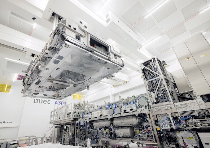
Imec and ASML have announced that the two companies have printed the first logic and DRAM patterns using ASML's experimental Twinscan EXE:5000 EUV lithography tool, the industry's first High-NA EUV scanner. The lithography system achieved resolution that is good enough for 1.4nm-class process technology with just one exposure, which confirms the capabilities of the system and that development of the High-NA ecosystem remains on-track for use in commercial chip production later this decade.
"The results confirm the long-predicted resolution capability of High NA EUV lithography, targeting sub 20nm pitch metal layers in one single exposure," said Luc Van den hove, president and CEO of imec. "High NA EUV will therefore be highly instrumental to continue the dimensional scaling of logic and memory technologies, one of the key pillars to push the roadmaps deep into the ‘angstrom era'. These early demonstrations were only possible thanks to the set-up of the joint ASML-imec lab allowing our partners to accelerate the introduction of High NA lithography into manufacturing."
The successful test printing comes after ASML and Imec have spent the last several months laying the groundwork for the test. Besides the years required to build the complex scanner itself, engineers from ASML, Imec, and their partners needed to develop newer photoresists, underlayers, and reticles. Then they had to take an existing production node and tune it for High-NA EUV tools, including doing optical proximity correction (OPC) and tuning etching processes.
The culmination of these efforts was that, using ASML's pre-production Twinscan EXE:5000 system, Imec was able to successfully pattern random logic structures with 9.5nm dense metal lines, which corresponds to a 19nm pitch and sub-20nm tip-to-tip dimensions. Similarly, Imec also set new high marks in feature density in other respects, including patterning of 2D features at a 22nm pitch, and printing random vias with a 30nm center-to-center distance, demonstrating high pattern fidelity and critical dimension uniformity.
The overall result is that Imec's experiments have proven that ASML's High-NA scanner is delivering on its intended capabilities, printing features at a fine enough resolution for fabricating logic on a 1.4nm-class process technology – and all with a single exposure. The latter is perhaps the most important aspect of this tooling, as the high cost and complexity of the High-NA tool itself (said to be around $400 million) is intended to be offset by being able to return to single-patterning, which allows for higher tool productivity and fewer steps overall.
Imec hasn't just been printing logic structures, either; the group successfully patterned DRAM designs as well, printing both a storage node landing pad alongside the bit line periphery for memory in a single exposure. As with their logic tests, this would allow DRAM designs to be printed in just one exposure, reducing cycle times and eventually costs.
![]()
9,5nm random logic structure (19nm pitch) after pattern transfer


"We are thrilled to demonstrate the world's first High NA-enabled logic and memory patterning in the joint ASML-imec lab as an initial validation of industry applications," said Steven Scheer, senior vice president of compute technologies & systems/compute system scaling at imec. "The results showcase the unique potential for High NA EUV to enable single-print imaging of aggressively-scaled 2D features, improving design flexibility as well as reducing patterning cost and complexity. Looking ahead, we expect to provide valuable insights to our patterning ecosystem partners, supporting them in further maturing High NA EUV specific materials and equipment."
Source: Imec


5 Comments
View All Comments
PeachNCream - Thursday, August 8, 2024 - link
Those are some HIGH-BS quotes so much that I feel like I'm drowning in pre-marketing hype!Has anyone tested this stuff for longevity or even functionality yet? Just because you have DRAM patterning doesn't mean it'll tolerate actual usage in not always favorable circumstances.
Jorgp2 - Thursday, August 8, 2024 - link
Did you understand a single word in this article?saratoga4 - Friday, August 9, 2024 - link
You're misunderstanding what was accomplished. These are tests of patterning resolution not the production of functional devices. The tests show that patterning is possible, nothing more. Youll have to wait for 1.4nn class transistors to ask about reliability.III-V - Friday, August 9, 2024 - link
That's not what they do; they just do R&D.Anymoore - Tuesday, August 13, 2024 - link
Are the line tips supposed to line up? It seems they move back and forth some nm.